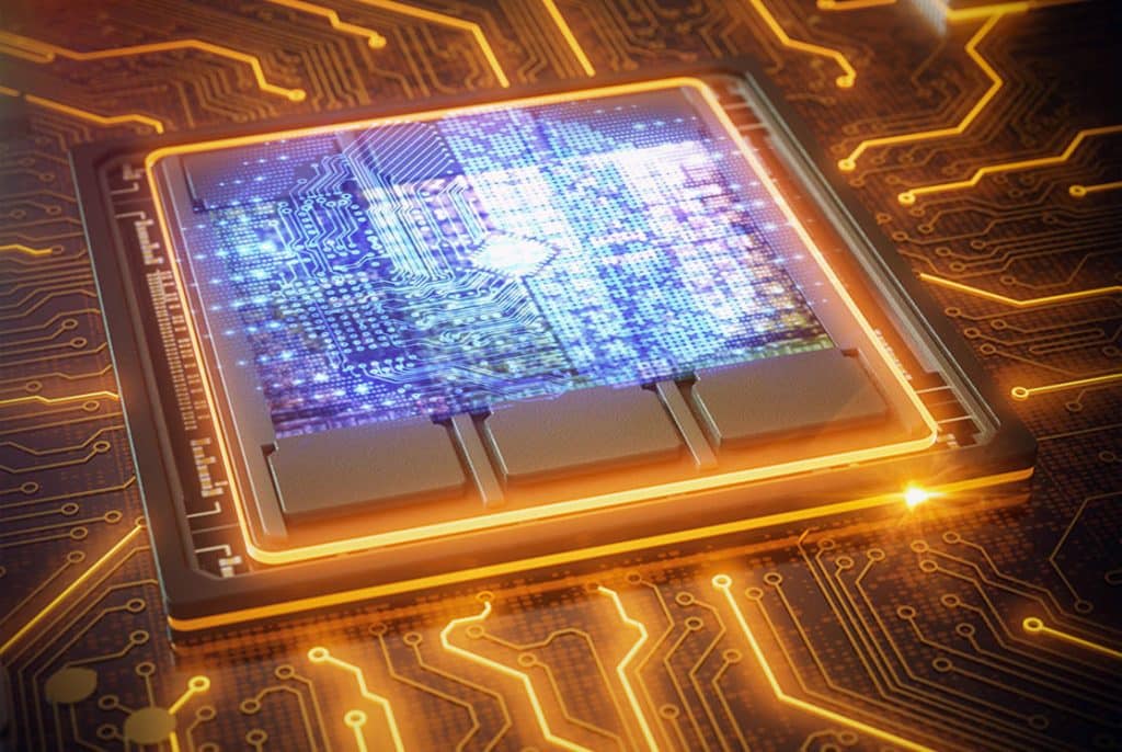
Advanced packaging including 2.5D, 3D-IC, fan-out wafer-level packaging and system-in-packaging.
Adaptive patterning, large fields, and unmatched resolutions for new packaging applications are all possible with the Multicolumn E-beam Platform. MEBL is capable of volume or batch production of System in Package (SiP), MEMS & Sensor Packaging, Fan Out Packaging, and 2.5D/3D IC Packaging. Enabling next generation very large and high-density interposers.
Multibeam technology is enabling game-changing improvements in:
Wafer-scale interposers (up to >80× larger)
Adaptable patterning (>10× higher bandwidth)
On-wafer die-die stitching (stitched die transcending reticle limit, with >98% energy reduction per bit transfer)
Our dynamic, adaptive direct write technology delivers:
Up to full-wafer interposers
Extremely high-density interconnects
Very high resolution; radial lines
Accommodation of high topology, common in 2.5D/3D
Wafer-Scale Heterogeneous Integration
Make die-die interconnect performance comparable to on-die interconnects.
Demand for higher computational power is stronger than ever, but combining chips together cohesively has been a struggle. Multibeam enables unparalleled heterogenous integration, combining chip power into one. This furthers efficiency that becomes a major boon for production
Large substrate size up to full wafer, no reticle stitching
Large DoF and surface flatness mapping cuts cost in stack-chip, 3D packaging and warped substrates
Adjustable patterning overcomes die-shift problem
E-beam writing radial lines and curves enables higher chip-chip interconnect density
Multibeam enables higher bandwidth, lower energy (for bit transfer chip-chip) with higher density and shorter data lines
Chip-chip interconnects comparable to on-chip interconnects
Photonics
E-beam lithography is essential for fabricating nanoscale photonic and electronic components that power next-generation applications
Enables ultra-high-resolution patterning critical for pushing the frontiers of SiPho device development
High pattern accuracy: Essential for fabrication of gratings and waveguides
Optical connections at the package and device level
Faster transition from research into scalable, market-ready solutions – scaling designs from prototype to mass production
Gratings
Photonics and laser-grating technologies are rapidly gaining prominence in the semiconductor industry as demand surges for high-performance data centers, AI/HPC (high-performance computing), advanced telecommunications (5G/6G), and precision sensing technologies such as LiDAR.
Wavelength-division multiplexing, and on-chip photonic components can help overcome electrical bandwidth and power limits, enabling faster data transfer, lower latency, and greater energy efficiency. Laser-fabricated or laser-assisted gratings are key enablers for wavelength filtering, beam steering, and coupling between optical and electronic domains, supporting next-generation network and sensing applications.
Despite these opportunities, manufacturing challenges remain. Scaling up precision laser grating production cost-effectively and ensuring reliability under high throughput also require advances in process control, defect mitigation, and metrology. Addressing these hurdles will be critical to fully harnessing photonics’ potential in future semiconductor ecosystems.
Mulibeam addresses these challenges by enabling:
Stitching-Free Gratings: Zero Phase Discontinuities – Continuous interferometer-tracked stage motion enables seamless grating fabrication across any device length—no field boundaries, no phase discontinuities, no degradation
Implementing efficient beam energy – At 5 kV, electron interaction volume is confined to the resist layer – Energy is deposited where it matters
For DFB grating fabrication on III-V substrates, low-kV operation isn’t just faster—it’s gentler on the device
Pitch Control: Sub-Angstrom Bragg Wavelength Accuracy – MEBL combines DAC deflection with continuous interferometer-tracked stage motion, adding an analog positioning component
Pitch is decoupled from DAC grid constraints—enabling true sub-angstrom pitch control without field scaling compromises
Pitch Stability – MEBL writes grating lines with minimal pitch-direction deflection (~10 µm vs. 1 mm)
15,000× pitch error reduction for height variation
Tolerant to wafer bow, chuck flatness, resist thickness variation
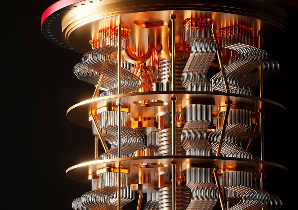
Quantum Technologies
Superconducting-qubit fabrication
Multibeam’s maskless, high-resolution patterning is a game-changer for rapidly prototyping and manufacturing quantum qubits and devices. For complex structures like quantum dots, superconducting qubits, and nanophotonic components, Multibeam EBL plays a key role in enabling device makers to significantly accelerate R&D cycles while maintaining high yield, and subsequently streamline the pilot to production ramp.
Multibeam technology is enabling game-changing improvements in:
Rapid Prototyping and Iteration: As a maskless technology, EBL allows for the direct writing of new, complex designs, cutting the time and cost associated with producing physical masks – an essential for iterating quantum device designs
Nanoscale Precision and Uniformity: Multibeam systems provide precise control over critical dimensions and placement, essential for maintaining qubit coherence and preventing device failures in superconducting, spin, or topological qubits
Complex Feature Generation: Multibeam technology enables the fabrication of complex, non-repeating, or high-density patterns (e.g., nanowires, intricate waveguides) needed for advanced quantum circuits and photonics
Scalable Manufacturing Capability: Multibeam systems enable full-wafer patterning at high speed, bridging the gap between small-scale prototyping and industrial production
Rapid Prototyping / High-Mix Production
Not every iteration of a project is perfect. However, with our e-beams, device makers can adapt to imperfections and make necessary changes on the fly. This provides a steep advantage compared to optical by removing the need to design new masks for each necessary change, perfect for purpose-built applications.
Rapid Prototyping: Digital printing and maskless patterning enable rapid prototyping for faster first article delivery and system productization
Accelerate the Path to Production: Speed up the development cycle for faster cycles of learning
Multi-Project Wafers: Enable high mix production with customizable patterning
Compound Semiconductor / Power Devices
E-beam is the top choice when it comes to reliability, stability and accuracy to pattern compound semiconductor material such as silicon carbide, gallium nitride, and other special materials.
Adapt to Topography: Easy accommodation for lack of flatness in SiC wafers
Smaller Gates: Easily meet < 60nm gate length requirements for next generation power amplifiers
Y-Axis Capability: 3D structures in high voltage, high power devices
High Resolution: < 50nm resolution on 200mm wafers
Mems & Sensors
The world isn’t flat, and neither are most die. With e-beam technology, MEBL can write on difficult die topography. Steps, valleys, and imperfections that can destroy a pattern pose less of an issue with Multibeam’s accuracy and FoV.
E-Beam Advantage: Large Depth of Focus (DoF) and high resolution
Wide Work Range: High Depth of Focus with variable working distance
Solution to Imperfections: System can handle wafer bow or distortions of hundreds of microns
Large Depth of Field: Columns have >10µm (DoF) for high aspect ratio (HAR) patterning
Secure Chip ID
Security is a must in a world with counterfeiters abound. Secure Chip ID is the leading anti-counterfeit capability, capable of hard-coding unique information into each chip seamlessly during routine wafer fabrication flow. Physically patterning IDs that are buried deep within the processing helps to enable essential system level security. By ensuring the provenance of critical IC components, Multibeam avoids vulnerabilities related to conventional approaches.
Embedded during device fabrication: Provides traceability to initial chip fabrication; Can’t be counterfeited
Guaranteed unique: Necessary to assure providence
Unique, tamper-proof, hardcoded: Completely non- volatile for life
Electrically readable: Usable for low-cost traceability or as part of secure chip architecture
Physically very small size: No impact on die size; Low cost
Your Dream, No Longer Just For Research
Multibeam’s unique multicolumn e-beam technology brings the high precision of e-beam direct writing to productivity levels that enable your applications to have:
100X
more productive than conventional e-beam
100X
larger writing field of view than optical lithography
100X
depth of Focus range of optical lithography
10X
more precision than laser direct write
All on a variety of substrate types and sizes. Multibeam systems empower IC leaders to make patterns that are impossible, difficult, or too expensive for mask-based solutions, with breakthrough time to market advantages.
Let's Discuss your Application
Get in touch with one of our experts to explore how we can accelerate the next generation of technology, together.


")


