
- MB Platform | Compact and Competitive
Our Products
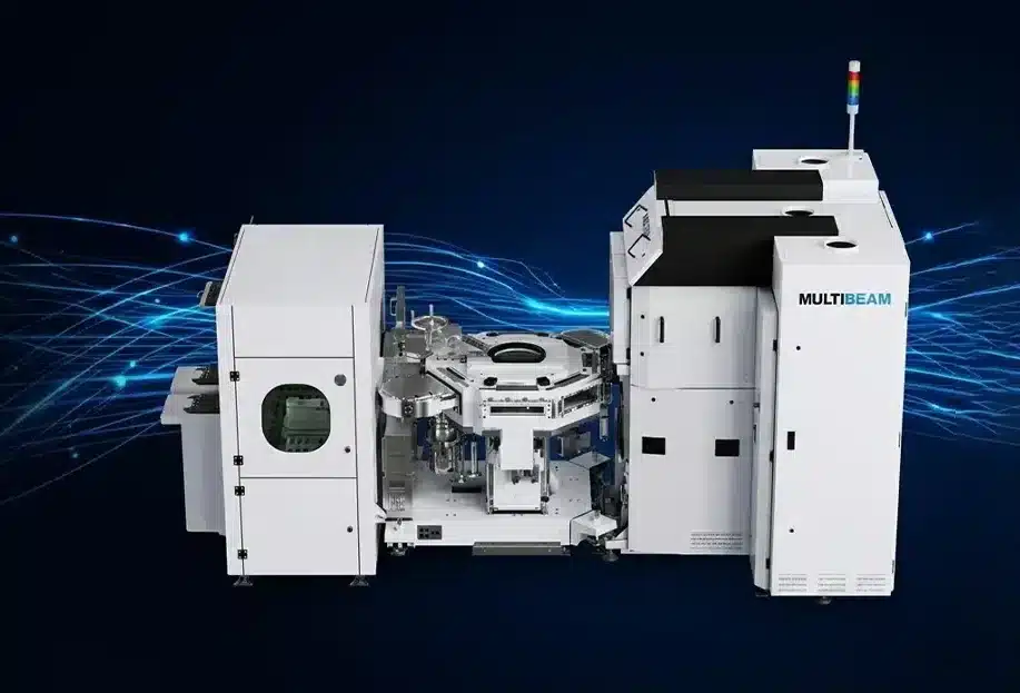
Multibeam’s high-productivity direct-write lithography systems are purpose-built to accelerate the prototype-to-production process with adaptable multi-column direct-write lithography for next generation advanced integration, photonics, quantum devices, compound semiconductors, and more.

- Lightning Fast Time to Market
MBX Platform
Multi-column E-Beam Lithography
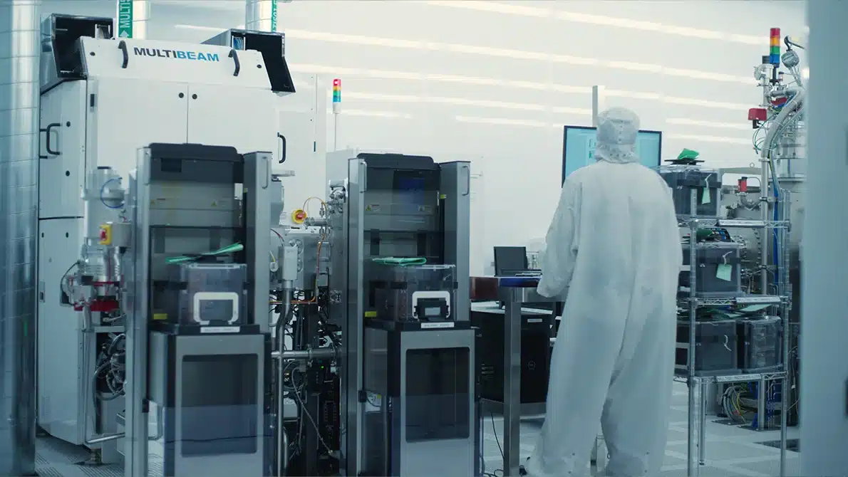
Our state-of-the-art MBX platforms deliver rapid design to wafer pattern and ultrafast cycles of learning. It allows for fast prototype & production for high-productivity volume manufacturing of custom, purpose-built patterns and advanced integration architectures.
Purpose-Built to Your Process
Every system can be configured to support your preferred substrate formats, materials, and target applications, enabling an optimized solution for your production needs.



Technical Specifications
| Technology | Multibeam® Multi-column E-Beam Lithography (direct-write) |
| Data Prep Software | Synopsys CATS software integrated within each Multibeam system |
| Substrate sizes (*Dependent on configuration) |
310mm panels 300mm wafers 200mm wafers 150mm wafers Contact us for 100mm & smaller wafers |
| Substrate types (*Dependent on configuration) |
Silicon, Silicon Carbide (SiC), Indium Phosphide (InP), Gallium Nitride (GaN), Gallium Arsenide (GaAs), Glass, Reconstituted wafers |
| Substrate handling (*Dependent on configuration) |
Fully automated handling, from wafer cassettes, SMIF pods, or FOUPs depending on model |
| Design file input | GDSII, OASIS, MULTIGON |
| Pattern types | Any pattern type or shape including Manhattan, curvilinear, radial |
| Write field/die size | up to Full wafer |
| Depth of focus range | 10 µm |
| Ability to handle topography | Handles bowed wafers, reconstituted wafers with topography > 100 µm |
| Adaptability | Adapts to underlying patterns, enabling mix-and-match with other lithography systems. Capable of adjusting patterns on interposers to compensate for chip-chip offsets, defects, etc. |
| Flexibility | Capable of individualization of every chip on wafer |
| Cycle time | No masks needed! Ready to begin writing within minutes of receiving design layout |
| Productivity | > 100X faster time to first pattern than Optical – no masks! >> 10X productivity compared to single E beam systems |
| Throughput | 1-2 wph typical per writing chamber Up to 25 wph per writing chamber (Secure Chip ID use case) |
| Acceleration Voltage | 5kV |
| Min Feature size | 30nm isolated; 50nm dense |
| Range of Feature Sizes | 30nm to >1 micron |
| Line Edge Roughness (LER) | < 10% of linewidth |
| Critical Dimension Uniformity (CDU) | < 10% of line-width typical |
| Overlay Error | < 30% of line-width typical |
| Capacity | Up to 3 writing chambers |
| Footprint | Single chamber 26.55 m², dual chamber 32.63 m² (these numbers include recommended service area) |
| Facility requirements | System is fully self-contained and isolated, no special facility requirements for temperature, vibration, or EMI |
Fully Automated
Multi-module capability (Up to 2x writing modules)
E-BEAM precision on a Fab-Worthy System
Fully isolated writing chamber (vibration, EMI, etc.)
Re-Innovating Maskless Semiconductor Lithography
About Multibeam Corporation
Headquartered in Sunnyvale, California, Multibeam engages in the design, manufacture, and sales of multi-column electron-beam lithography (MEBL) systems that enable rapid prototype to production capabilities for advancing heterogeneous chiplet integration, silicon photonics, quantum computing, and other rapidly growing applications.
At the heart of Multibeam technology is an array of miniature e-beam columns that provide a maskless and high-throughput platform for writing nanoscale IC patterns seamlessly across full wafers. This solves key limitations widely recognized with e-beam lithography, transforming it from a mere R&D curiosity to an incredible fab tool for production.
Headquarter Office - Silicon Valley, U.S.A
+1 (408) 980-1800
Have an inquiry? Call Us
1213 Innsbruck Drive Sunnyvale, CA 94089, U.S.A.
Visit our HQ