Traditional manufacturing workflows often slow innovation through lengthy mask cycles, design lock-in, and limited opportunities for experimentation.
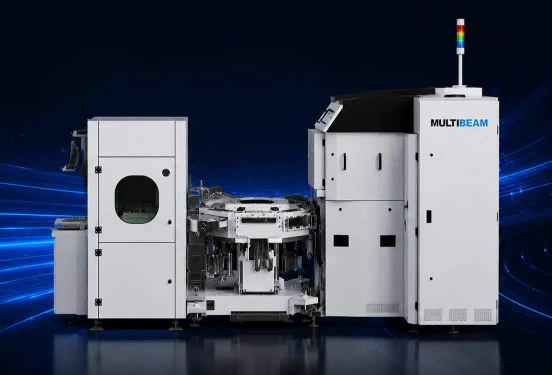
MBX-300 changes the equation.
- Rapid Learning
- Rapid Iteration
- Rapid Scale
MBX-300: Accelerate the Future of Semiconductor Manufacturing
The next era of semiconductor innovation won’t be defined by who can build the biggest fab. It will be defined by who can learn, iterate, and scale the fastest.
The MBX-300™ is a second-generation multi-column e-beam lithography platform engineered to dramatically accelerate the path from concept to production. By combining adaptable direct-write patterning with ample substrate flexibility, MBX-300 enables manufacturers to develop, optimize, and scale next-generation devices faster than ever before.
The future belongs to those who can learn faster
Whether you’re building next-generation advanced packaging architectures, photonic integrated circuits, quantum devices, or compound semiconductors, MBX-300 empowers teams to move from design to wafer, and from pilot to production, with unprecedented speed and precision.
BUILT FOR WHAT'S NEXT
Purpose-Built for the Industry's Most Demanding Applications
Advanced Packaging
As AI, high-performance computing, and chiplet architectures drive unprecedented integration complexity, manufacturers need lithography solutions that can adapt as quickly as their designs evolve.
MBX-310 or MBX-300 enables:
- High-density interconnect patterning
- Advanced 2.5D and 3D integration
- Adjustable lithography & process flexibility
- Rapid design modifications without mask re-spins
- Faster development cycles for heterogeneous integration
Photonics
As data centers, AI infrastructure, telecommunications, and sensing applications transition toward optical connectivity, precision and scalability become critical.
MBX-200, MBX-150, or MBX-300 delivers:
- High-uniformity optical gratings and waveguides
- DFB laser and photonic integrated circuit fabrication
- Curvilinear patterning for complex optical structures
- Rapid design iteration for device optimization
- Faster transition from R&D to manufacturing
Quantum Computing
Quantum technologies demand precision, flexibility, continuous experimentation, and the ability to scale novel device designs to production rapidly.
MBX-300, MBX-200 supports:
- Rapid prototyping of novel quantum architectures
- High-resolution nanoscale patterning
- Multiple design experiments on a single substrate
- Accelerated process development cycles
- Consistent manufacturing performance for scale-up
- Faster learning loops between design, fabrication, and characterization
One Platform. Vast Flexibility.
The semiconductor landscape is diversifying rapidly. New materials, new device architectures, and new form factors require manufacturing platforms that can evolve alongside innovation.
MBX-300 is designed to handle a broad range of substrate formats and materials within a single production-ready platform.
Supported Substrate Sizes
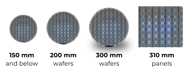
- 150mm and smaller
- 200mm wafers
- 300mm wafers
- 310mm panels
Supported Materials (in addition to standard Silicon)
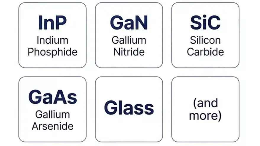
- Silicon (Si)
- Indium Phosphide (InP)
- Gallium Nitride (GaN)
- Silicon Carbide (SiC)
- Gallium Arsenide (GaAs)
- Glass
Learn Faster. Commercialize Faster.

By enabling direct-write manufacturing at production-relevant throughput levels, teams can:

Test more ideas

Run more experiments

Evaluate more device variations

Optimize designs faster

Reduce development risk

Shorten time-to-market
The result is a dramatically accelerated learning cycle - allowing manufacturers to make better decisions, sooner.
A TURNKEY SOLUTION FOR EVERY STAGE
From Prototype to Production - on the Same Platform
Innovation shouldn’t require changing tools as you scale.
MBX-300 enables a seamless path from early development through pilot production and high-volume manufacturing, reducing technology transfer risk while accelerating commercialization.
Manufacturers can:
- Validate concepts quickly
- Refine designs continuously
- Scale successful devices efficiently
- Reduce process complexity
- Accelerate yield learning
When every development cycle matters, the ability to move faster becomes a competitive advantage.

Multibeam Corporation: Innovating Maskless Semiconductor Lithography
Headquartered in Sunnyvale, California, Multibeam engages in the design, manufacture, and sales of multi-column electron-beam lithography (MEBL) systems that enable rapid prototype to production capabilities for advancing heterogeneous chiplet integration, silicon photonics, quantum computing, and other rapidly growing applications.
At the heart of Multibeam technology is an array of miniature e-beam columns that provide a maskless and higher-throughput platform for writing nanoscale IC patterns seamlessly across full wafers. This solves key limitations widely recognized with e-beam lithography, transforming EBL from an R&D tool into a production solution.
- Faster Learning
- Faster Development
- Faster Commercialization
The Next Generation of Manufacturing Agility
The semiconductor industry is entering an era where speed of learning determines speed of innovation. MBX-300 empowers manufacturers to iterate faster, adapt faster, and bring breakthrough products to market faster.
Meet the MBX-300™ — the next generation of high-productivity multi-column e-beam lithography.

© 2026 Multibeam Corporation. All Rights Reserved.